Superconducting filter design in Ansys HFSS
In the last entry of this blog, I talked about some of the aspects of transmission lines that are useful for those working with microwave signals. The discussion was mainly focused on the physical intuition behind distributed-element circuits, and how parameters such as a line length $L$, dielectric propagation constant $\varepsilon_r$, and characteristic wave impedance $Z_0$ affect the propagation of signals down a transmission line.
I got a lot of good feedback from that discussion, so I want to supplement it with a more practical leaning. Today, I want to show different transmission line architectures and how to quantitatively extract $\varepsilon_r$ and $Z_0$ using finite-element simulations. I will then show how to use this information to build filters. By the end of the post, I will also show some experimental tests that I did on a low-pass filter and how it compares with simulation.
If you leave this post wishing to know more, I recommend checking the classic reference on the topic - Pozar, David M. Microwave engineering. Its content is not trivial to digest, but our discussion here should give a good headstart.
Table of Contents
- Table of Contents
- Finite-element simulation of transmission lines
- Assembling transmission lines into filters
- Conclusion
Finite-element simulation of transmission lines
Before start drawing a transmission line, think what it should look like. Is it a coaxial line, a coplanar waveguide, or something new altogether? Any pair of conductors interacting through extended lengths can transmit signals, so let your imagination run wild. But also keep this in mind when analyzing complex circuits, because any two unassuming conductors can become a critical leakage channel for your signals.
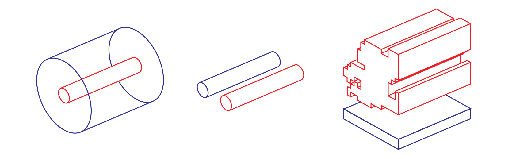
For simplicity, this post will focus on a coaxial architecture where the center conductor is printed on a sapphire chip, a common setup in 3D superconducting circuits. The figure below shows the Ansys HFSS design from which we will extract the parameters $\left(Z_0, \varepsilon_r\right)$. One end of the center conductor is touching one wall of the waveguide, and the other end is left open (load $Z_L \to \infty$).
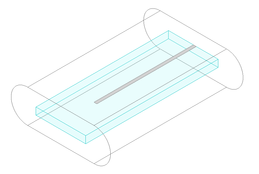
We start a Terminal Network analysis and select the wall touching the inner conductor as a Terminal Wave port, using the waveguide as a reference conductor (in other words, the ground). We then simulate the one-port impedance $Z_{11}(f) = Z_{in}(f)$ as a function of frequency, which can be modeled as
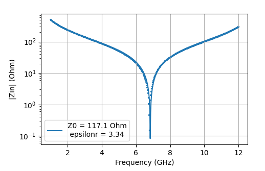
\[Z_{in}(f) = Z_0\frac{Z_L + jZ_0\tan\left(\frac{2\pi}{c}\sqrt{\varepsilon_r}fL\right)}{Z_0 + jZ_L\tan\left(\frac{2\pi}{c}\sqrt{\varepsilon_r}fL\right)} \, \xrightarrow{Z_L\to \infty} -\frac{jZ_0}{\tan\left(\frac{2\pi}{c}\sqrt{\varepsilon_r}fL\right)}.\]Here $c$ is the speed of light and $j$ is the imaginary unit. Knowing $L$ from the design, it is possible to extract both parameters from a single fit - $Z_0$ defines the magnitude of $Z_{in}$, whereas $\varepsilon_r$ defines the frequencies of poles and zeros.
The simulation data is extracted as a .txt and fitted to $Z_{in}(f)$, as seen in the figure below, giving $Z_0 = 117\,\Omega$ and $\varepsilon_r = 3.34$. So there you go, a characterized transmission line! I shared the simulation file, results and code in a github repo. One tip is to not include poles in the fitted data, since these regions are most prone to numerical error.
Assembling transmission lines into filters
As an example, I will design the simplest filter in the textbook - a lowpass Butterworth filter of 3rd order. This filter can be translated into transmission lines as shown in the figure below (again, see Pozar for more details).
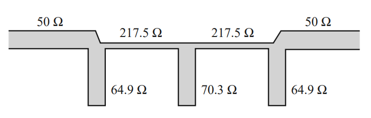
These values assume the filter is normalized to $Z_0 = 50\,\Omega$, meaning the lines connected to each port should have this characteristic impedance. The length of every line section is $\lambda/8$, where $\lambda$ is the wavelength of the cutoff frequency $f_c$. So, the physical length of the $k$-th section must be $L_k = \lambda_k/8 = c/8f_c\sqrt{\epsilon_{r,k}}$, and the line width should be adjusted to match the desired $Z_{0,k}$.
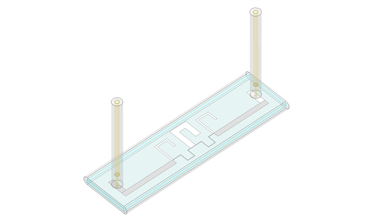
The simulation and fitting step must be repeated for every line section to calibrate the target $L_k$ and $Z_{0,k}$. This step can be quite tedious, but some architectures have helpful analytical formulas. Once each part is individually calibrated, they can be assembled as a filter, as in the next figure. Now you can define two ports, one for each end of the filter, and measure the transmission $S_{21}$. It should behave as a low-pass with cutoff at $f_C$. In my simulation I made a few practical adjustments: the lines are curved for compactness, and the ports are given by Pogo pins touching the on-chip lines.
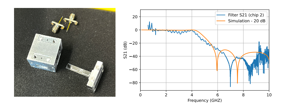
This design was fabricated using superconducting aluminum for the filter and the waveguide, as can be seen in Figure X, and the $S_{21}$ was measured at cryogenic temperatures using a Vector-Network Analyzer. As can be seen in the plot, the experimental curve is very similar to the HFSS simulation, validating our recipe!
Conclusion
The simulations and results shown here are quite simple, but a powerful example for designing any type of filter. The same method can be adapted for stepped-impedance or coupled-resonator filters, high- or band-pass, CPW or microstripline architectures. Whatever your target filter is, I hope this post will be a good starting point. 加油!