Disentangling transmission lines
Transmission lines (TLs) are the backbone of any radio-frequency (RF) circuit. For anyone using RF signals to control quantum systems such as superconducting circuits, the transmission lines will be the ones connecting the grubby, classical outside world with the low-noise environment of the dilution refrigerator.
Most of the time, TLs such as SMA cables are just bought off the shelf and used without much thought - not even with a glance at the specs sheet. This is almost aways perfectly fine. But sometimes when working with superconducting circuits, understanding the nuances of TL physics is necessary to engineer the systems more accurately. For example, on-chip filters are often designed solely based on a bunch of connected TLs. And that’s when the false familiarity of everyday use leads to confusion.
My purpose is to give the basic tools researchers need to design transmission lines in superconducting circuits. This knowledge could be used to design qubit control lines, on-chip filters and resonators, or simply help better understand how electromagnetic fields behave at circuit level. I will split the story into two post: the first one will explain some of the physics behind TLs. The second post will show how to design filters in superconducting circuits using finite-element simulations.
As a guideline, in this post I will comment on a few confusion points that I sometimes see in the laboratory. We will build some intuitive understanding of transmission lines, and explore some relevant circuit equations.
Table of Contents
- Table of Contents
- Transmission lines are not just DC wires
- TLs don’t need a closed loop to carry signals
- Transmission lines have real impedances - which doesn’t mean they are lossy
- Conclusion
Transmission lines are not just DC wires
What is the difference between the two images below?
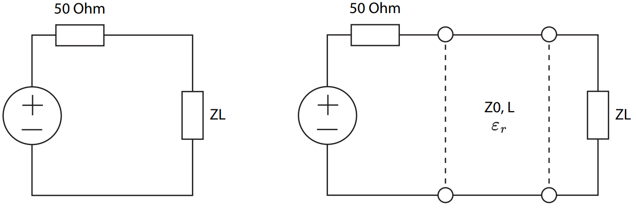
The image on the left is a common DC circuit. The voltage along each wire is constant by definition, following the electrostatics assumption that every point of a conductor shares the same potential.
The right image shows a very similar circuit, but the connection between the source and the load is done through a transmission line. The only physical difference between both models is that we lift the electrostatic assumption. Let me explain why.
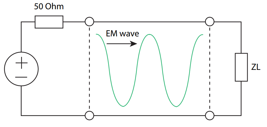
If the signal generated by the source is fast-changing, it takes finite time to travel through the line. The voltage of the conductor doesn’t have time to settle, forming a travelling wave. Since the wave propagation is not instantaneous, we need to take into account the line length L and the signal propagation speed characterized by the relative permittivity $\varepsilon_r$. That’s when the transmission line model comes in hand.
Following this argument, it is easy to see that the transmission line behaves as a DC wire at the limit of short lengths L. Conversely, this approximation is also valid when the signal is composed of low frequencies, meaning the minimum wavelength $\lambda$ is much larger than L.
TLs don’t need a closed loop to carry signals
This is another confusion that arises from comparing RF circuits with their DC counterparts. Let’s check the circuit again, but now assuming that the circuit is open.
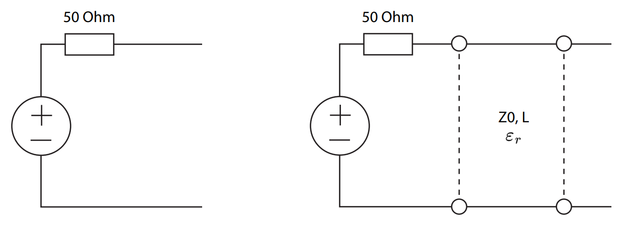
We know the open DC wires simply don’t carry any current. The voltage drop at the terminals is equal to the voltage provided by the source.
Now assume the source sends a high-frequency signal through a long line. We know this signal will take some time to travel to the other end and “feel” the open circuit. This means that, at any point in time:
- The voltage at the open end is not necessarily equal to the source, and
- The current provided by the source is not necessarily zero
In other words, even if the circuit is open, it is possible to send a voltage or current signal down the line.
This thought experiment also reveals another very interesting effect. As the source now provides non-zero voltage and current, it is as if the transmission line has “transformed” the open load $Z_L \to \infty$ into a finite input impedance $Z_{in} < \infty$.
This impedance transformation follows the notorious formula:
\[Z_{in}(f) = Z_0\frac{Z_L + jZ_0\tan(\frac{2\pi}{c}\sqrt{\epsilon_r}fL)}{Z_0 + jZ_L\tan(\frac{2\pi}{c}\sqrt{\epsilon_r}fL)}\]Here $Z_{in}$ is the impedance perceived at the start of the TL, $f$ is the frequency of a spectral component of the signal, $Z_L$ is an arbitrary load at the end of the line, $c/\sqrt{\varepsilon_r}$ is the signal propagation speed, $L$ is the line length and $Z_0$ is the characteristic impedance of the line. We explore the last property in the next point.
From this formula, we can verify one of our previous conclusions: when $L\ll \lambda = \frac{c}{\sqrt{\varepsilon_r}f}$, the transmission line approximately behaves as a DC wire since $Z_{in}(f) \to Z_L$ for any frequency.
Transmission lines have real impedances - which doesn’t mean they are lossy
We just learned that transmission lines have an extra parameter called its characteristic impedance $Z_0$, which comes in the formula for $Z_{in}$.
A common misunderstanding is thinking that $Z_0$ represents a circuit element, and that the line should be somehow lossy when $\textnormal{Re}(Z_0) \neq 0$. But that is not true. An open circuit is lossless for any $Z_0$ (check that $Z_L \to \infty$ means $Z_{in}$ is always imaginary). So what is the actual meaning of $Z_0$?
While $Z_0$ is an impedance like any other, it actually quantifies the relation between the electric and magnetic fields $\vec{E}$ and $\vec{H}$ travelling down between the two wires of the TL:
\[Z_0(x) = \frac{\|\vec{E}(x)\|}{\|\vec{H}(x)\|}\]For a homogeneous line, $Z_0$ is independent of the position $x$. We can show that $|\vec{E}|\propto V^+$ and $|\vec{H}|\propto I^+$, where $V^+$ and $I^+$ are the voltage drop and a current waves travelling in the same direction as the electromagnetic wave (denoted as $+$). We can then show that:
\[Z_0 = \frac{V^+(x)}{I^+(x)}\]The impedance is the same if the wave is travelling in the opposite direction (labelled as $-$), so:
\[Z_0 = -\frac{V^-(x)}{I^-(x)}\]The minus signal accounts for the current flipping directions. At any point $x$, the voltage is given by the sum $V^+(x) + V^-(x)$, while the current is given by $I^+(x) - I^-(x)$. The input impedance at that point is therefore
\[Z_{in}(x) = \frac{V^+(x) + V^-(x)}{I^+(x) - I^-(x)}.\]With a bit more of derivation and assuming harmonic oscillations, we can derive the previously shown equation for $Z_{in}$.
So what is $Z_0$? A wave impedance. Its “reality” is not associated to losses through Ohms law, as with regular resistors. Instead, it quantifies how a wave propagates through space. But some food for thought: if the energy carried by a wave with impedance $Z_0$ is never reflected back and leaves the circuit (imagine an infinite transmission line), then this propagation can in fact be interpreted as a loss to a resistor $Z_0$. This is equivalent to assuming $Z_L = Z_0$, leading to $Z_{in} = Z_0$.
Conclusion
I hope to have help you build some intuition on how transmission lines behave and how they build up on DC circuits. Although my explanations are not meant to be comprehensive, they should provide an initial understanding for those who want to venture further into the matter. But most importantly: always remember the difference between the load impedance $Z_L$, the characteristic impedance $Z_0$ and the input impedance $Z_{in}$.
In the next post, I will show how to measure and design all of the properties of a transmission line, and show how it can be used to design filters. Until then!